What Factors Should IoT PCB Designers Take Into Account Circuit Diagram In this comprehensive video, Peter from Tech Explorations takes you through the entire process of designing a custom IoT PCB using KiCad 9. From schematic cr Select the Right PCB Materials. PCB substrate choice can impact cost, manufacturability and device performance. Consider factors like: Number of layers - 2 to 6 layer PCBs are commonly used for IoT devices depending on complexity.; Board thickness - Typically between 1.6 mm to 2.4 mm. Thicker boards provide more rigidity.; Material - FR-4 is the most common PCB material. IoT PCB design teams will eventually need to work with a manufacturer to get a board produced. Bringing a manufacturer into a collaborative process is a huge value add that can reduce turn times and help you spot DFM errors early. A cloud-based system for IoT PCB design lets everyone on a team see a full set of design and fabrication data.

Hey there! I'm Ryan, an Electrical Design Engineer at Flux AI, where I help push the boundaries of PCB design with AI-powered tools.My background spans power electronics, camera systems, and embedded hardware, with hands-on experience designing power supplies, high-speed MIPI interfaces, and real-world PCB validation.. Before Flux, I worked at Skydio, designing power systems and camera However, the PCB design stage is the most crucial for a successful outcome. PCB Design: It is easy to fix bugs and other issues related to code by revising the firmware. However, once a PCB is manufactured and assembled, revising it for mistakes involves substantial amounts of time and cost involvement. Therefore, when designing PCBs for IoT or IoT Hardware systems. Autodesk Eagle . Schematic design. PCB design. Programming. In this course we will start by teaching absolute basics of Autodesk Eagle, so that you can efficiently and easy follow the process of creating a useful and beautiful IoT device, which you can manufacture, build and use in many different ways.
Powered PCB Design with Flux Circuit Diagram
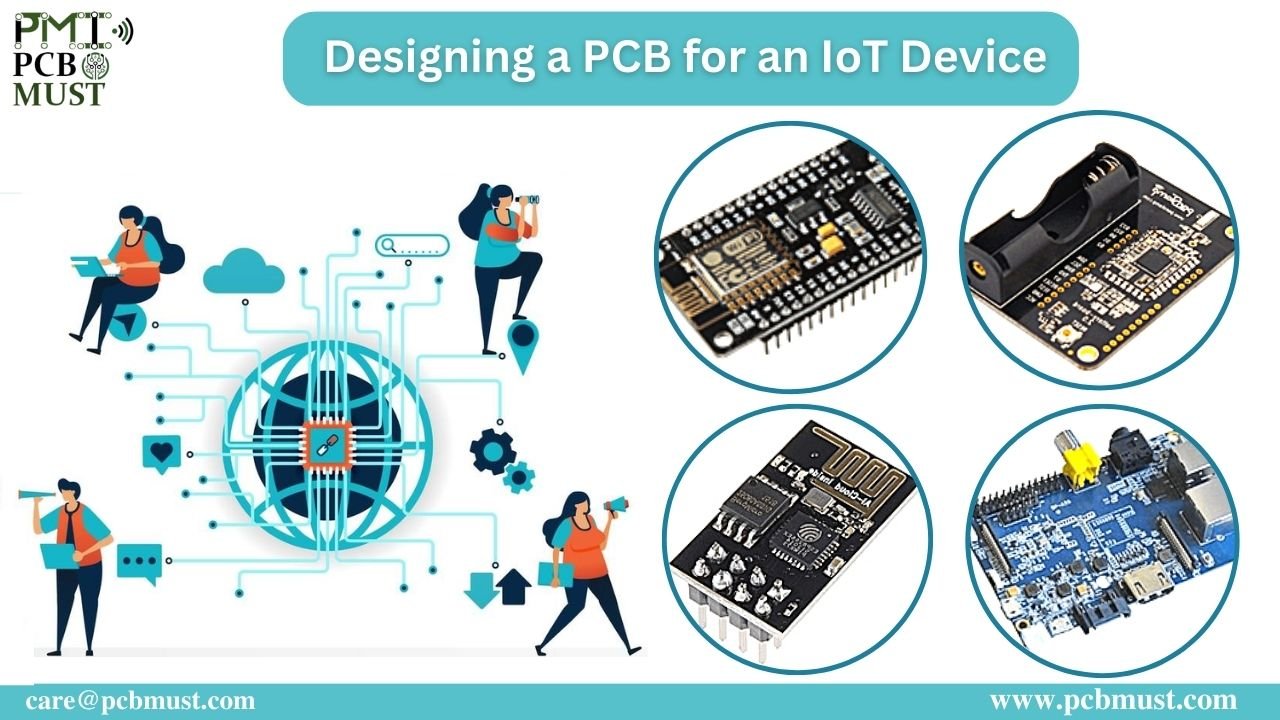
IoT Design: Basic Building Blocks. At its core, an IoT device has a couple of key components that define it: sensors, a wireless connectivity block, and a power management block. The main challenge in successful IoT design is having them all work together smoothly. Sensors. Firstly, sensors focus on gathering data from the outside world.
Complete step-by-step PCB design process going through the schematic, layout, and routing of a ESP32-based PCB including USB in the new KiCAD 7. All the way Designing a PCB for IoT applications is a complex and challenging task that requires careful planning, attention to detail, and a deep understanding of both the application requirements and the principles of PCB design.By following this step-by-step approach, you can create a PCB that not only meets the functional needs of your IoT device but also ensures reliability, scalability, and efficiency.